EV technology is the future of the automobile industry that continuously sees rapid advancements in battery and fast charger technology. Without sacrificing charging time, research and development is underway to ensure that the size of the battery is smaller and power consumption during charging time is minimal.
EV technology is the future of the automobile industry that continuously sees rapid advancements in battery and fast charger systems. Without sacrificing charging time, research and development is underway to ensure that the size of the battery is smaller and power consumption during charging time is minimal.
Solar PVs, wind turbines, and energy storage systems have three-phase inverters that are used as an interface between the active distribution network and the distributed energy resources (DERs). Nowadays, conventional bulky transformers with more compact solid-state transformers (SSTs) also require three-phase inverters to feed the loads. Usually, three-phase four-wire inverters are required when DERs and SSTs are used to supply unbalanced loads for providing an additional path for the zero-sequence current of the loads.
Technology using silicon carbide-based semiconductor devices has an upper hand due to its various advantages when compared with conventional EV chargers. Traditionally, 50-kW EV chargers have a distribution transformer weighing 1,000 kg and a separate charging unit weighing 200 to 600 kg. Additionally, this weight (transformer and charging system) requires installation on a concrete slab.
Each module consists of a three-level boost PFC stage and 1,600-V to 400-V isolated DC/DC stage. These modules are designed to be stackable and support up to 450 kW and future EVs of 800 V.

conventional neutral leg. (b) With the improved neutral leg by removing C (Source: Link)
Compared with conventional chargers, using SiC, a 50-kW charger weighs only 100 kg and can be wall-mounted, offering about 4× the power using the same system footprint and reducing the installation cost.
Control design
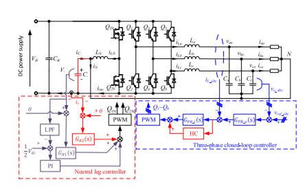
The above circuit diagram shows the control strategy of the three-phase four-wire inverter along with the proposed neutral leg. In the above diagram, the proposed neutral leg is shown in the first part and the closed-loop control of the three-phase four-wire inverter is shown in the second part.
The proposed neutral leg requires only two additional controllers: the power-decoupling controller GR2(s), which is used in decoupling the second-order ripples from the DC bus, and the harmonic compensator (HC), which is used to compensate the harmonics in the load currents. The following section explains the control of the SiC-based neutral leg.
Control of the proposed neutral leg
A neutral-current controller and power-decoupling controller are present in the control of the proposed neutral leg.
Neutral-current controller
This controller works similarly to the controller of the conventional neutral leg. Thus, the same controller can be directly adopted by the proposed neutral leg for the conventional neutral leg. Here, a simple PI controller connected in parallel with a resonant controller is applied, assuming that the neutral current contains only the fundamental component. Here, a low-pass filter (LPF) is adopted to get the average voltage of C– and to extract the DC component of V–:
Here, ωc is the cutoff frequency of the LPF. Harmonic components at 100 Hz and beyond are supposed to filter out, so ωc is set as 50 rad/s. A PI controller can be applied to regulate the average value of V– to Vdc/2.
From the above equation, kp is the proportional gain and ki is the integral gain ki.
To ensure that the neutral current is provided through the neutral inductor Ln instead of the capacitor C– , a resonant controller GR1(s) is applied:
Here, ω is the fundamental angular frequency, ξ1 is the cutoff frequency of the resonant controller, and KR1 is the resonant gain of the controller. Gain GR1(s) is almost zero everywhere, but resonant frequency ω is not zero. V– is to be measured as the feedback of GR1(s) to regulate its fundamental component to be zero.
Power-decoupling controller
Another resonant controller GR2(s) is applied in the power-decoupling controller.
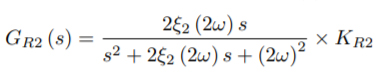
From the above equation, ξ2 defines the cutoff frequency, KR2 is the resonant gain of the controller, and GR2(s) has the resonant peak at 100 Hz. DC bus current is, the feedback of GR2(s), and the second-order components is are controlled to be zero.
The proposed neutral leg can provide neutral currents and can reduce DC bus ripples simultaneously, with the neutral-current controller and the power-decoupling controller being paralleled together.
Control of three-phase inverters
The three-phase four-wire inverter works in standalone mode to supply the unbalanced loads with balanced three-phase voltages. Hence, the AC voltage closed-loop control is performed with the inner control loop. Three phases are independently controlled by proportional-resonant current and voltage controllers:
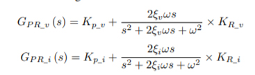
From the above equation, Kp_v is the proportional gain of the voltage and Kp_i is the current controller; KR_v is the resonant gain of the voltage and KR_i is the current controller; and ξv and ξi is the coefficient of the cutoff frequency. Also, the second-order harmonics need to be compensated by the current controller because of the voltage variation of the neutral point caused by power-decoupling controller GR2(s). Therefore, as shown above, the HC is connected in parallel with GP R_i (s) to compensate for the harmonics at 100 Hz:
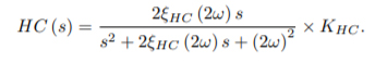
From the above equation, ξHC is the cutoff frequency of HC(s) and KHC is the resonant gain of the controller.
DC bus voltage requirements
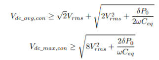
From the above equations, Vdc_avg,con is the average DC bus voltage, Vdc_max,con is the maximum DC bus voltage caused by the unbalanced second-order power ripple with the conventional neutral leg, and Ceq is the equivalent DC bus capacitance.
DC capacitance
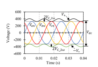
For three-phase inverters that supply AC voltages of 230 Vrms, 1,200-V semiconductor switches (Si IGBTs or SiC MOSFETs) are selected. Hence, the DC bus voltage should not exceed 1,200 V. The DC bus capacitance must be designed in such a way that the DC bus voltage does not exceed 750 V.
As shown in the first figure, Cdc is the total sum of small film capacitors that are placed close to the switches, reducing the voltage overshoot and switching harmonics. Because the value of Cdc is negligible (10 µF), the major part of the bus capacitance is the capacitance of the neutral leg. However, the equivalent DC bus capacitance is reduced in view of the series connection of the capacitors.
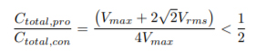
From the above equation, Ctotal,pro and Ctotal,con are the total capacitance required by the proposed and conventional legs, respectively.
Conclusion
After comparing with the conventional neutral leg, the SiC-based neutral leg provides neutral currents and reduces second-order DC bus ripples. The following parameters are achieved by making use of SiC-based neutral legs:
- Output power: 50 kW
- Input voltage: 2,400 VAC
- Output voltage: 200–500 VDC
- Peak efficiency: 97.6%
- Power factor: ≥98
- Input current THD: ≤5%