Designers must consider processing temperatures, producibility, and solder joint integrity of every component as well as higher I/O connectors. This article looks at ways to enable smaller component footprints for high-density PCBs.
As electronics continue to become smaller and faster, the supporting components must develop first to enable smaller footprints. Increasing the density and reducing the size gives manufacturers less room for error, and better processing methods must be developed.
Processing higher density connectors on a printed circuit board assembly create complications that must be addressed. Designers must consider processing temperatures, producibility, and solder joint integrity of every component. The increased density is due to the demand for a higher I/O connector in the same space once occupied by a much lower I/O connector.
The traditional through-hole or surface mount connectors have reached a limit on the number of signals (pins per square inch) that can be effectively used in these applications. This is where connector manufacturers have considered utilizing BGA, solder crimp, and solder charge designs to reduce the component footprint.
Solderability
For a double row connector, solderability issues are typically easy to address. Not to mention, if there is an issue then it can be addressed with a rework by using a simple soldering iron to correct a solder joint. However, on multi-row connectors, this process becomes more involved, and properly processing the connector the first time becomes increasingly important.
Some of the common issues that can cause a bad solder joint are:
- Solder paste volume
- Stencil size
- Incorrect solder oven temperature profile
- PCB flatness
With the issues listed above, there isn’t a one-size-fits-all solution because each manufacturing set-up is unique. Some of the variances that must be considered are the equipment being used, solder paste (brand and chemical makeup), and the application (board design, component density, etc.).
Connector Solutions For High-Density I/O Needs
One of the solutions that connector manufacturers have used for high-density applications is a BGA setup. BGA applications use a spherical solder ball attached to the component lead in order to provide more solder without using a heavy paste.
Solder charges, as found on Samtec’s SEARAY™ High-Density Open-Pin-Field Arrays, are a similar solution to a BGA, but provide better edge bonding of the connector to the PCB pad.
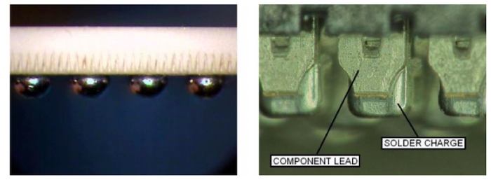
Figure 1. Solder balls on BGA vs. solder charges on Samtec’s SEAF8 / SEAM8
Another unique difference of the solder charge on the SEARAY™ 0.8 mm (SEAF8 / SEAM8 series) is the alternating pitches of 0.80mm and 1.20mm. This design can afford the board designer additional trace routings between rows.
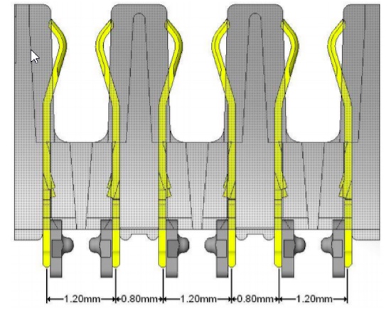
Figure 2. Alternating pitch of the SEAF8 / SEAM8
Keys to Achieving Better Solder Joints During Processing
As a rule, it is best to follow the manufacturer’s processing guidelines for the highest success in soldering a part to a PCB. Some manufacturers will provide a PCB footprint, stencil layout and thickness, solder screen printing process, component placement, proper oven profiling, and even rework considerations.
Footprint and Stencil
Connector manufacturers often offer the PCB designer the ability to download the PCB footprint and the stencil layout and thickness. Samtec offers more than 200,000 symbols and footprints for download in popular EDA tools such as Altium, Circuit Studio, Eagle, Fusion 360, and more.
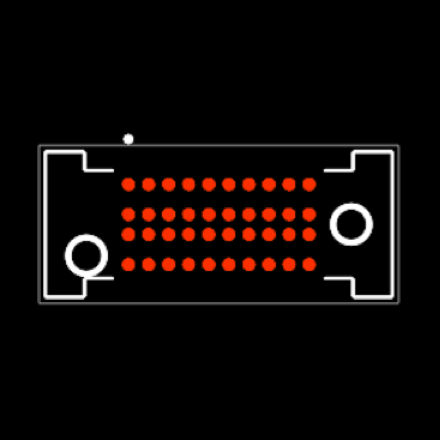
Figure 3. SEAF8 PCB footprint
By utilizing the provided footprint and stencil layout, the PCB designer has a higher probability of achieving proper solder joints.
Solder Screen Printing Process
Solder pad coverage is critical for a proper solder joint, and the pad should be completely covered. For this reason, the aperture size in the stencil is intentionally larger than the pad on the PCB. This is to ensure that the solder charge on the SEAF8 (or connector) comes into contact with the solder paste as shown in Figure 4.
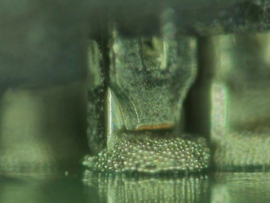
Figure 4. Solder charge location relative to the solder print with good contact between paste and solder charge.
If the solder paste does not properly cover the solder charge, then proper wetting will not be achieved. Automated inspection is used to ensure proper solder coverage on the PCB. It is recommended that any solder pad assembly not completely covered be rejected, cleaned, and reprinted.
Placing the Component
Automated pick and place equipment will ensure the proper placement of the components. For proper solder wetting, it is important that the Z-axis dimension will fully seat the solder charges onto the surface of the PCB.
As the solder charges reflow in the oven, the weight of the connector will cause the connector to settle onto the board, or close to it, after processing. This phenomenon helps reduce any coplanarity in the connector as shown in Figures 5 and 6 below.
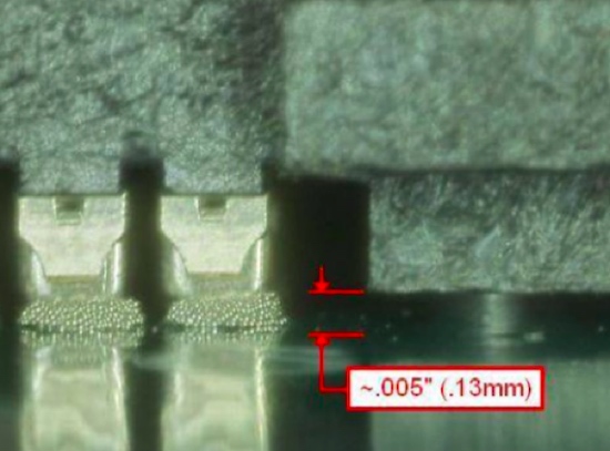
Figure 5. SEAF8 insulator housing fully seated prior to processing.
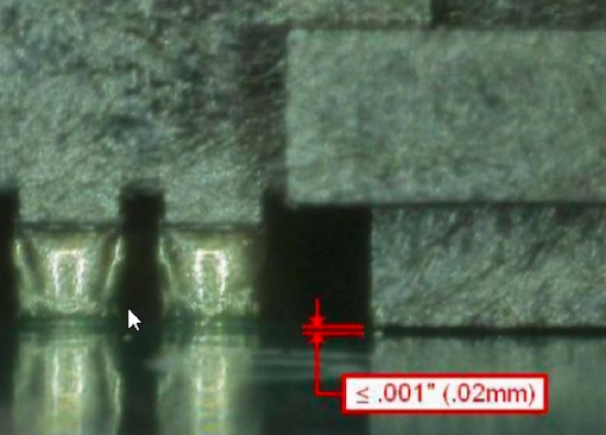
Figure 6. SEAF8 insulator housing fully seated after reflow.
Proper Oven Profiling
At this point, most surface mount components should be capable of handling lead-free solder reflow profiles as described in IPC/JEDEC J-STD-020. This specification requires that the components must be capable of withstanding a peak temperature of 260°C as well as 30 seconds above 255°C.

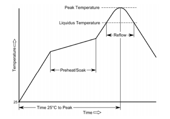
Figure 7. Samtec Recommended Temperature Profile Ranges (SMT)
A low-level oxygen environment, typically achieved through nitrogen gas infusion, in the reflow process will help increase the wettability of the soldering surfaces. For a high-density connector similar to the SEAF8 / SEAM8, it is recommended that solder processing is only completed in a nitrogen-rich environment.
Properly profiling the fully populated PCB assembly is vital. The reflow process that forms the solder joints can often be overlooked but is it critical to ensure the solder joints are properly formed.
To ensure that the solder charges are reaching the desired temperature, it is recommended that a thermocouple be placed through the back of the board into the center of the connector and placed on the outside edge. This will ensure that the reflow profile parameter of the solder paste manufacturer will be achieved.
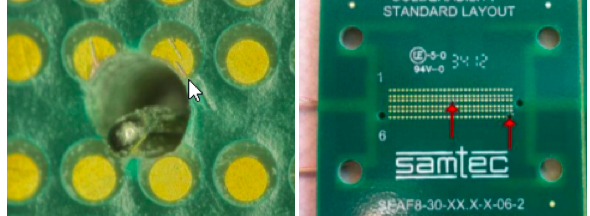
Figure 8. Thermocouple placement for oven profile.
Increasing Importance of Proper Processing
While no process can be without flaws, using a proper processing setup will eliminate the need for reworks, scrap, and lower profits. This importance will continue to increase as electronics get smaller and their components get denser. This is why Samtec provides footprints and stencil layouts for all of its connector series and provides information on how to properly process its more complex product series.
Industry Articles are a form of content that allows industry partners to share useful news, messages, and technology with All About Circuits readers in a way editorial content is not well suited to. All Industry Articles are subject to strict editorial guidelines with the intention of offering readers useful news, technical expertise, or stories. The viewpoints and opinions expressed in Industry Articles are those of the partner and not necessarily those of All About Circuits or its writers.


