The LM25145 is a 42-V synchronous buck controller. This post mainly covers its pinout, datasheet, application circuit and more details about LM25145.
The LM25145 is a 42-V synchronous buck controller. This post mainly covers its pinout, datasheet, application circuit and more details about LM25145.
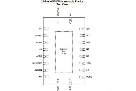
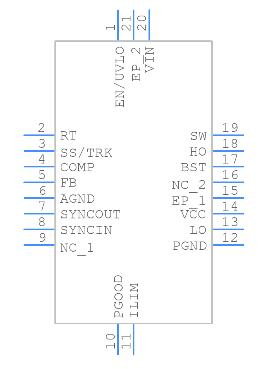
LM25145RGYR Pinout
Symbol
LM25145 Symbol
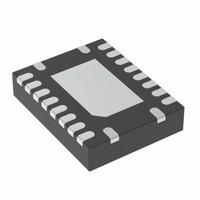
Footprint

LM25145 Footprint
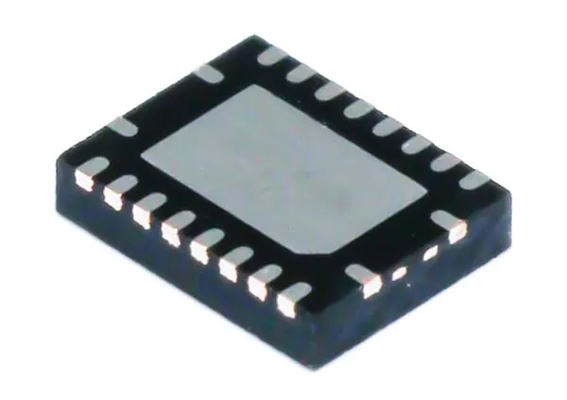
3D Model

LM25145 3D Model
The LM25145 is a 42-V synchronous buck controller that features all of the functions necessary to implement a high-efficiency step-down power supply with an output voltage ranging from 0.8 V to 40 V. The voltage-mode control architecture uses input feedforward for excellent line transient response over a wide VIN range. Voltage-mode control supports the wide duty cycle range for high input voltage and low dropout applications as well as when a high voltage conversion ratio (for example, 10-to-1) is required. Current sensing for cycle-by-cycle current limit can be implemented with either the low-side FET RDS(on) or a current sense resistor. The operating frequency is programmable from 100 kHz to 1 MHz.
The LM25145 drives external high-side and low-side NMOS power switches with robust 7.5-V gate drivers suitable for standard threshold MOSFETs. Adaptive dead-time control between the high-side and low-side drivers is designed to minimize body diode conduction during switching transitions. An external bias supply can be connected to the VCC pin to improve efficiency in high-voltage applications. A user-selectable diode emulation feature enables discontinuous conduction mode operation for improved efficiency and lower dissipation at light-load conditions.
Versatile synchronous buck DC-DC controller
Wide input voltage range of 6V to 42V
Adjustable output voltage From 0.8V to 40V
Meets EN55022 / CISPR 22 EMI standards
Lossless RDS(on) or shunt current sensing
Switching frequency from 100kHz to 1MHz
SYNC In and SYNC out capability
40ns Minimum on-time for high VIN / VOUT ratio
140ns minimum off-time for low dropout
0.8V Reference with ±1% feedback accuracy
7.5V Gate drivers for standard VTH MOSFETs
14ns Adaptive dead-time control
2.3A Source and 3.5A sink capability
Low-side soft-start for pre-biased start-up
Adjustable soft-start or optional voltage tracking
Fast line and load transient response
Voltage-mode control with line feedforward
The high gain-bandwidth error amplifier
A precision enables input and open-drain power good indicator for sequencing and control
Inherent protection features for robust design
Hiccup mode overcurrent protection
Input UVLO with hysteresis
VCC and Gate drive UVLO protection
Thermal shutdown protection with hysteresis
VQFN-20 Package with wettable flanks
Telecom infrastructure
Factory automation
Test and measurement
Industrial motor drives
The LM25145 functional block diagram is shown below:
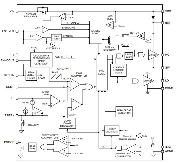
LM25145RGYR Functional Block Diagram
The following figure shows a typical application circuit and efficient performance of LM25145:
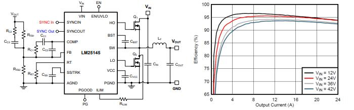
LM25145 Typical Application Circuit and Efficiency Performance, VOUT = 5 V, FSW = 225 kHz
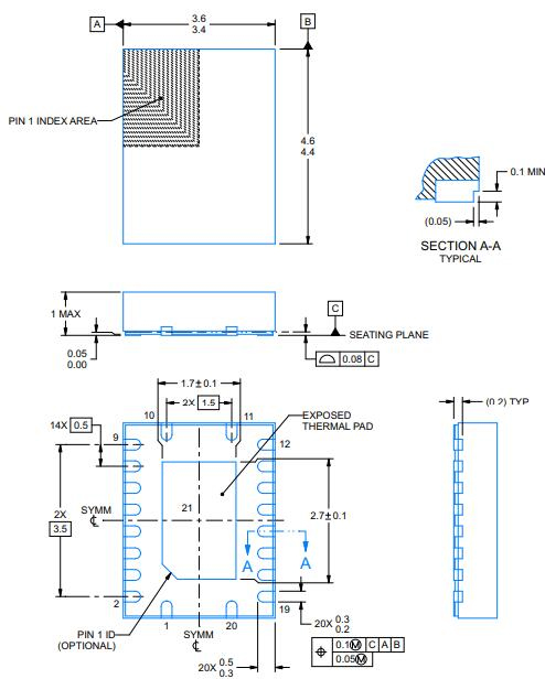
LM25145 Package
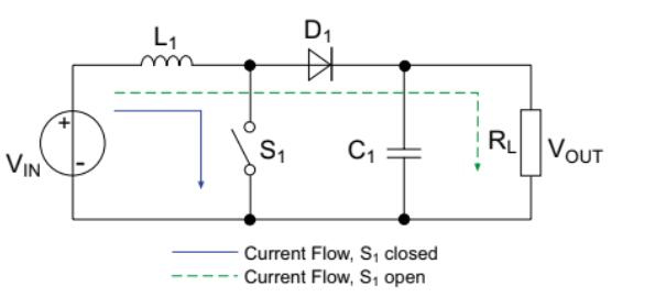
A buck or step-down converter is a DC/DC switch mode power supply designed to buck (or lower) an unregulated DC supply's input voltage to a stabilized lower output voltage. Buck converters are highly appreciated for their extraordinarily high efficiency, which can easily surpass 95 per cent when compared to ordinary voltage regulators. The simplified circuit schematic below depicts how current flows across the circuit during a buck converter switching event.
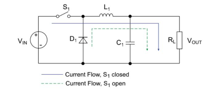
Buck Converter Circuit
A boost converter is a DC/DC switch mode power supply designed to boost (or enhance) an unregulated DC supply's input voltage to a stabilized higher output voltage. A boost converter, like a buck converter, uses an inductor, diode, capacitor, and power switch to adjust the output voltage, but they are organized differently. The simplified circuit schematic below depicts how current travels through the circuit during a boost converter switching event.
Boost Converter Circuit
The output voltage of a boost converter is controlled by the mark-space ratio of the PWM signal to be equal to or greater than V in. Because power is conserved, a boost converter that supplies three times the input voltage can only supply one-third of the current that it pulls from the supply. Boost converters, on the other hand, are highly popular in battery-powered devices, where a pair of batteries may give 3V but must power a 5V circuit.
| Attribute | Value |
|---|---|
| Lifecycle Status | ACTIVE (Last Updated: 3 days ago) |
| Factory Lead Time | 6 Weeks |
| Mounting Type | Surface Mount, Wettable Flank |
| Package / Case | 20-VFQFN Exposed Pad |
| Surface Mount | YES |
| Number of Pins | 20 |
| Operating Temperature | -40°C~125°C TJ |
| Packaging | Tape & Reel (TR) |
| JESD-609 Code | e3 |
| Pbfree Code | yes |
| Part Status | Active |
| Moisture Sensitivity Level (MSL) | 2 (1 Year) |
| Number of Terminations | 20 |
| Terminal Finish | Matte Tin (Sn) |
| Additional Feature | ADJUSTABLE OUTPUT VOLTAGE FROM 0.8 V TO 40 V |
| Terminal Position | QUAD |
| Terminal Form | NO LEAD |
| Peak Reflow Temperature (Cel) | 260 |
| Terminal Pitch | 0.5mm |
| Time@Peak Reflow Temperature-Max (s) | NOT SPECIFIED |
| Base Part Number | LM25145 |
| Attribute | Value |
|---|---|
| Function | Step-Down |
| Number of Outputs | 1 |
| Output Type | Transistor Driver |
| Input Voltage-Nom | 24V |
| Analog IC - Other Type | SWITCHING CONTROLLER |
| Output Configuration | Positive |
| Voltage - Supply (Vcc/Vdd) | 6V~42V |
| Control Features | Enable, Frequency Control, Ramp, Soft Start |
| Input Voltage (Min) | 6V |
| Topology | Buck |
| Control Mode | VOLTAGE-MODE |
| Frequency - Switching | 100kHz~1MHz |
| Input Voltage (Max) | 42V |
| Control Technique | PULSE WIDTH MODULATION |
| Synchronous Rectifier | Yes |
| Height | 1mm |
| Length | 4.5mm |
| Width | 3.5mm |
| Thickness | 900μm |
| RoHS Status | ROHS3 Compliant |
Download datasheets and manufacturer documentation for