NPN & PNP Transistors explained - electronics engineering
Bipolar Transistors - BJT PNP Med Power
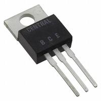
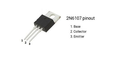
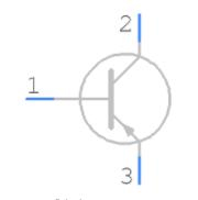
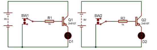
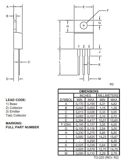
2N6107 is a PNP transistor and has a gain value of 30 to 150; this value determines the amplification capacity of the transistor. In this post, we are going to unlock its pinout, datasheet, equivalent, how to use and more details about 2N6107.