What is CLOCK GENERATOR? What does CLOCK GENERATOR mean? CLOCK GENERATOR meaning & explanation
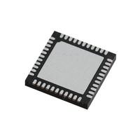
IC CLK BUFFER PLL 44QFN
The Si5346 is a dual DSPLL version in a smaller package. Each DSPLL has access to any of the four inputs and can provide low jitter clocks on any of the device outputs. Each DSPLL supports independent free-run, holdover modes of operation, as well as automatic and hitless input clock switching. Furthermore, Huge range of Semiconductors, Capacitors, Resistors and IcS in stock. Welcome RFQ.