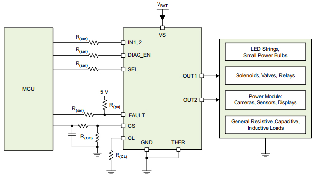
Quick Links

TPS2H160BQPWPRQ1 Description

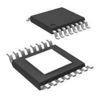
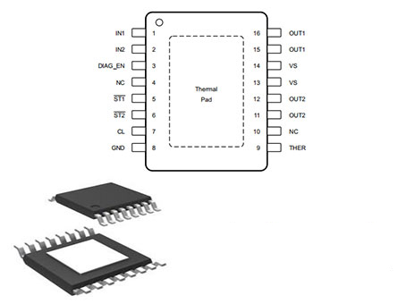
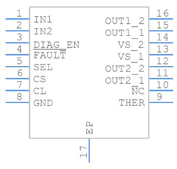
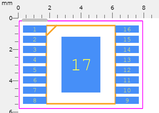
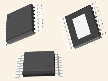
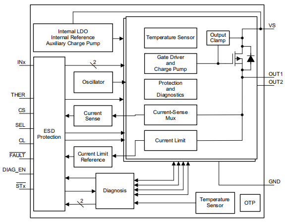
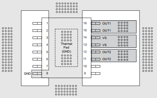
The TPS2H160BQPWPRQ1  is a smart high-side switch with a built-in charge pump and dual-channel NMOS power   FETs . The load may be intelligently controlled thanks to full diagnostics and high-accuracy current-sense features. The configurable current-limit mechanism considerably improves the system's overall reliability. The open-drain digital output (version A) and the current-sense analog output (version B) have different diagnostic reporting (version B).

The gadget uses an open-drain structure to implement the digital fault report in version A. The device pulls STx down to GND when a failure occurs. To match the microcontroller supply level, a 3.3- or 5-V external pullup is necessary. Each channel's digital status can be reported individually or collectively by connecting the STx pins together.

For version B, high-accuracy current sense improves diagnostic accuracy without requiring further calibration. 1 / K(CS) of the load current can be provided by a single integrated current mirror. The mirrored current enters the CS-pin resistor and transforms into a voltage signal. K(CS) is a constant value that remains constant regardless of temperature or supply voltage. A large linear range of 0 to 4 V provides for more accurate real-time load-current monitoring. With VCS pullup voltage, the CS pin can also notify a fault (H).

Applications can set the current-limit value using the external high-accuracy current limit. When there is an overcurrent, the device increases system reliability by effectively clamping the inrush current. By lowering the size of PCB traces and connectors, as well as the capacity of the previous power stage, the device can reduce system costs. In addition, the device has an inbuilt current restriction with a preset setting.

To protect itself from inductive loads (relays, solenoids, and valves), the gadget uses an active clamp between drain and source. On the high-side switch, both the energy of the power supply and the load is dissipated during the inductive switching-off cycle. When the clamp is active, the device also optimizes the switching-off slew rate, which aids system design by reducing the effects of transient power and EMI.

The TPS2H160BQPWPRQ1 is a smart high-side switch for low-wattage bulbs, LEDs, relays, solenoids, heaters, and sub-modules, among other resistive, inductive, and capacitive loads.


TPS2H160BQPWPRQ1 Pinout

The following figure is TPS2H160BQPWPRQ1 Pinout.

Pinout


Pin Number Pin Name Description
7 CL Adjustable current limit. Connect to device GND if external current limit is not used.
3 DIAG_EN Enable-disable pin for diagnostics; internal pulldown
8 GND Ground pin
1 IN1 Input control for channel 1 activation; internal pulldown
2 IN2 Input control for channel 2 activation; internal pulldown
4,10 NC No internal connection
5 ST1 Open-drain diagnostic status output for channel 1
6 ST2 Open-drain diagnostic status output for channel 2
9 THER Thermal shutdown behavior control, latch off or auto-retry; internal pulldown
15,16 OUT1 Output of the channel 1 high side-switch, connected to the load
11,12 OUT2 Output of the channel 2 high side-switch, connected to the load
13,14 VS Power supply
  Thermal pad Connect to device GND or leave floating

TPS2H160BQPWPRQ1 CAD Model

The following figures are TPS2H160BQPWPRQ1 Symbol, Footprint and 3D Model.

Symbol

Footprint

3D Model

TPS2H160BQPWPRQ1 Features

• Qualified for Automotive Applications

• AEC-Q100 Qualified With the Following Results:

– Device Temperature Grade 1: –40°C to 125°C Ambient Operating Temperature Range 

– Device HBM ESD Classification Level H2

– Device CDM ESD Classification Level C4B

• Functional safety capable

– Documentation available to aid functional safety system design 

• Dual-Channel 160-mΩ Smart High-Side Switch With Full Diagnostics

– Version A: Open-Drain Status Output 

– Version B: Current-Sense Analog Output

• Wide Operating Voltage 3.4 to 40 V

• Ultralow Standby Current, < 500 nA

• High-Accuracy Current Sense:

– ±17% Under >25-mA Load

• Adjustable Current Limit With External Resistor ±15% Under >500-mA Load

• Protection:

– Short-to-GND Protection by Current Limit (Internal or External)

– Thermal Shutdown With Latch-Off Option and Thermal Swing

– Inductive Load Negative Voltage Clamp With Optimized Slew Rate

– Loss of GND and Loss of Battery Protection 

• Diagnostic:

–  Overcurrent  and Short to Ground Detection

– Open-Load and Short-to-Battery Detection

– Global Fault for Fast Interrupt

• 16-Pin Thermally-Enhanced PWP Package

Specifications

Attribute Value
Lifecycle Status ACTIVE (Last Updated: 3 days ago)
Factory Lead Time 12 Weeks
Mounting Type Surface Mount
Package / Case 16-PowerTSSOP (0.173, 4.40mm Width)
Surface Mount YES
Number of Pins 16
Operating Temperature -40°C~125°C TA
Packaging Tape & Reel (TR)
Series Automotive, AEC-Q100
JESD-609 Code e4
Pbfree Code yes
Part Status Active
Moisture Sensitivity Level (MSL) 3 (168 Hours)
Number of Terminations 16
ECCN Code EAR99
Resistance 155mOhm
Terminal Finish Nickel/Palladium/Gold (Ni/Pd/Au)
Terminal Position DUAL
Terminal Form GULL WING
Number of Functions 2
Supply Voltage 13.5V
Base Part Number TPS2H160
Number of Outputs 2
Attribute Value
Output Type N-Channel
Supply Voltage-Min (Vsup) 4V
Interface On/Off
Output Configuration High Side
Voltage - Supply (Vcc/Vdd) Not Required
Switch Type General Purpose
Nominal Input Voltage 40V
Ratio - Input:Output 1:1
Voltage - Load 3.4V~40V
Fault Protection Current Limiting (Adjustable), Over Temperature
Turn On Time 90 µs
Output Peak Current Limit-Nom 2.5A
Rds On (Typ) 155m Ω
Turn Off Time 90 µs
Built-in Protections TRANSIENT; OVER CURRENT; THERMAL; UNDER VOLTAGE
Output Current Flow Direction SOURCE
Height 1.2mm
Length 5mm
Width 4.4mm
Thickness 1mm
REACH SVHC No SVHC
RoHS Status ROHS3 Compliant
Lead Free Lead Free

TPS2H160BQPWPRQ1 Functional Block Diagram

The TPS2H160BQPWPRQ1 Functional Block Diagram is shown as follows.

Functional Block Diagram

TPS2H160BQPWPRQ1 Typical Application

The following figure shows an example of the external circuitry connections based on the version-B device.

Typical Application Schematic

Typical Application Diagram


• VVS range from 9 V to 16 V

• Load range is from 0.1 A to 1 A for each channel

• Current sense for fault monitoring

• Expected current-limit value of 2.5 A

• Automatic recovery mode when thermal shutdown occurs

• Full diagnostics with 5-V MCU

• Reverse-voltage protection with a blocking diode in the power-supply line

TPS2H160BQPWPRQ1 Layout

TJ must be less than 150°C to avoid thermal shutdown. The thermal impedance of the HTSSOP package is excellent. The  PCB  layout, on the other hand, is critical. A good PCB design can improve heat transfer, which is critical for the device's long-term durability.

• Maximize the copper coverage on the PCB to increase the thermal conductivity of the board. The major heat flow path from the package to the ambient is through the copper on the PCB. Maximum copper is extremely important when there are not any heat sinks attached to the PCB on the other side of the package.

• Add as many thermal vias as possible directly under the package ground pad to optimize the thermal conductivity of the board.

• All thermal vias should either be plated shut or plugged and capped on both sides of the board to prevent solder voids,  To ensure reliability and performance, the solder coverage should be at least 85%.


Without a GND Network

Without a GND network, tie the thermal pad directly to the board GND copper for better thermal performance.

Layout Example Without a GND Network


With a GND Network

With a GND network, tie the thermal pad as one trace to the board GND copper.

Layout Example With a GND Network

TPS2H160BQPWPRQ1 Applications

• Dual-Channel LED Drivers, Bulb Drivers

• Dual-Channel High-Side Switches for SubModules

• Dual-Channel High-Side Relay, Solenoid Drivers

TPS2H160BQPWPRQ1 Package

The TPS2H160BQPWPRQ1 Package is shown as follows.

Package

TPS2H160BQPWPRQ1 Manufacturer

Texas Instruments Incorporated (TI) is an American technology corporation based in Dallas, Texas, that creates and manufactures semiconductors and integrated circuits for electronic designers and manufacturers around the world. Based on sales volume, it is one among the top ten semiconductor businesses in the world. Analog chips and embedded processors, which account for more than 80% of the company's revenue, are the company's main focus.

Datasheet PDF

Documents

Download datasheets and manufacturer documentation for   

Frequently Asked Questions

FAQ

What is a TPS2H160BQPWPRQ1?
A smart high-side switch with a built-in charge pump and dual-channel NMOS power FETs.
What are the benefits of the TPS2H160BQPWPRQ1?
Full diagnostics and high-accuracy current-sense features.
What greatly improves the systems overall reliability?
Configurable current-limit mechanism.
What does the TPS2H160BQPWPRQ1 use to implement the digital fault report in version A?
Open-drain structure.
What is required to match the microcontroller supply level?
3.3- or 5-V external pullup.
How can each channels digital status be reported?
Individually or collectively.
What improves diagnostic accuracy for the TPS2H160BQPWPRQ1?
High-accuracy current sense.
What can be provided by the TPS2H160BQPWPRQ1?
1 / K(CS) of the load current can be provided by a single integrated current mirror.
What enters the CS-pin resistor and transforms into a voltage signal?
Mirrored current.
What is the linear range of the TPS2H160BQPWPRQ1?
0 to 4 V.
What can the CS pin notify a fault?
VCS pullup voltage.
What does the TPS2H160BQPWPRQ1 have?
Applications can set the current-limit value using the external high-accuracy current limit.
What does the device do when there is an overcurrent?
The device increases system reliability.
What does the TPS2H160BQPWPRQ1 have?
An inbuilt current restriction with a preset setting.
What does the TPS2H160BQPWPRQ1 use to protect itself from inductive loads?
An active clamp between drain and source.
What does the high-side switch use to protect itself from inductive loads?
The energy of the power supply and the load is dissipated during the inductive switching-off cycle.
What does the TPS2H160BQPWPRQ1 do when the clamp is active?
The switching-off slew rate.
Tags -
Share this post